What This Document Is
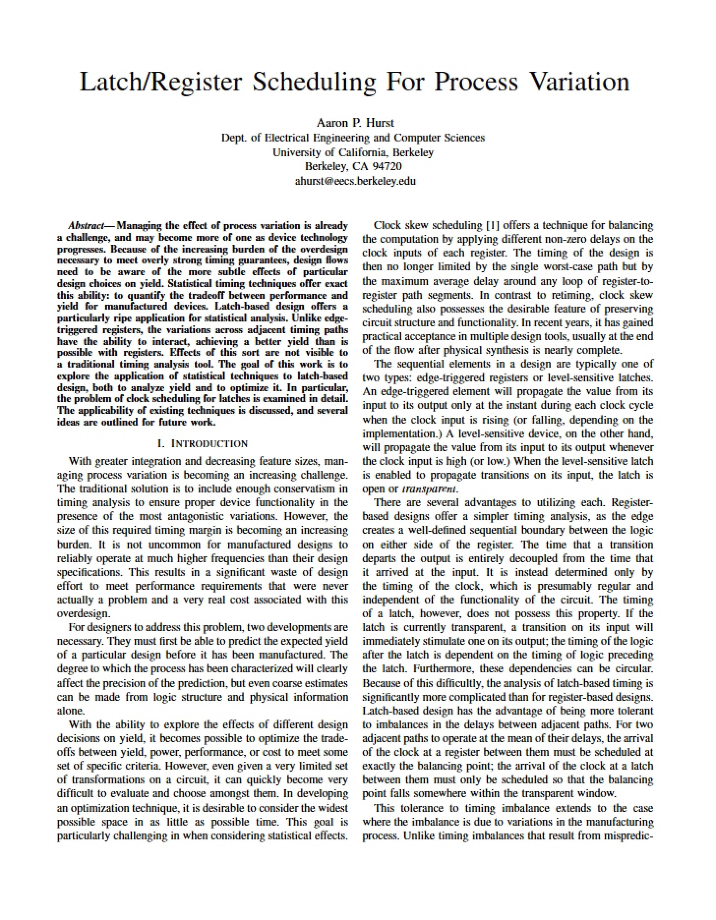
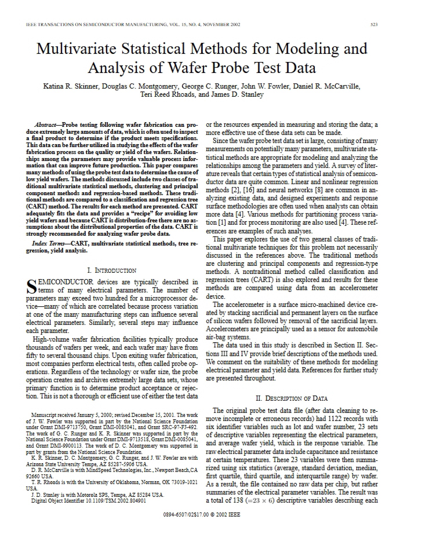
This document presents a focused investigation into the complexities of state machine design within the realm of digital logic and computer-aided design. Specifically, it delves into the critical processes of determinization and minimization of state machines – foundational concepts for creating efficient and reliable digital systems. It appears to be a research paper originating from academic work at the University of California, Berkeley, and published in IEEE Transactions on Semiconductor Manufacturing. The document utilizes a technical writing style common in advanced engineering studies.
Why This Document Matters
This material is essential for advanced undergraduate and graduate students in electrical engineering, computer engineering, and related fields. It’s particularly valuable for those specializing in VLSI design, digital systems, or formal verification. Professionals working on hardware design, embedded systems, or logic synthesis will also find this a useful resource for deepening their understanding of state machine optimization techniques. It’s best utilized when tackling complex design projects or seeking to improve the performance of existing digital circuits.
Topics Covered
* State Machine Determinization
* State Minimization Techniques
* Pattern-Dependent Variation Analysis
* Chemical-Mechanical Polishing (CMP) impact on circuit performance
* Modeling of polishing behavior based on layout patterns
* Analysis of pattern density, area, pitch, and perimeter/area effects
* Spatial variation in semiconductor manufacturing processes
What This Document Provides
* A detailed exploration of methods for characterizing and modeling pattern dependencies in semiconductor manufacturing.
* Discussion of test mask designs for efficient data collection related to polishing processes.
* Comparative analysis of pattern-dependent variation models for different polishing pads.
* Insights into the dominant factors influencing pattern-dependent variation in oxide CMP.
* A technical framework for understanding the relationship between layout patterns and dielectric layer thickness.