What This Document Is
This document contains lecture text from ELENG 130: Integrated-Circuit Devices, offered at the University of California, Berkeley. Specifically, it represents the core concepts presented in Lecture #2 of the course. It delves into the fundamental electronic properties of silicon, a cornerstone material in semiconductor device fabrication. The material is designed to build a foundational understanding of how charge carriers behave within silicon and how these behaviors are critical to device operation.
Why This Document Matters
This lecture text is invaluable for students currently enrolled in ELENG 130, or those reviewing introductory solid-state electronics. It’s particularly helpful for understanding the theoretical underpinnings of semiconductor behavior *before* tackling more complex circuit analysis or device design. Students preparing for quizzes or exams on semiconductor physics will find this a useful resource to solidify their grasp of key principles. It’s best utilized alongside attendance in the lecture itself and in conjunction with assigned readings.
Topics Covered
* The nature of charge carriers in silicon (electrons and holes)
* The relationship between material properties and electrical resistivity
* Methods for modulating carrier concentration within a semiconductor
* The bond model explaining electron and hole creation
* The concept of intrinsic carrier concentration
* The energy band model and its application to silicon
* The valence and conduction bands and the significance of the band gap
What This Document Provides
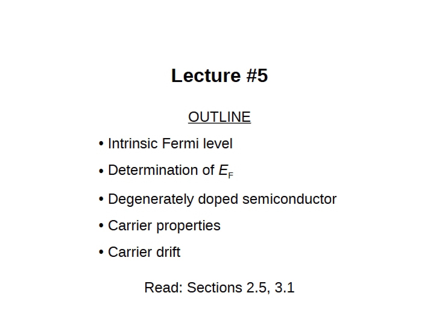
* A detailed outline of the lecture’s key discussion points.
* Visual representations illustrating the behavior of electrons and holes within a silicon lattice.
* Definitions of essential terms related to semiconductor physics.
* An explanation of how atomic energy levels transition into energy bands within a crystalline structure.
* A conceptual overview of the energy band diagram and its components.
* A summary of the core concepts presented in the lecture.