What This Document Is
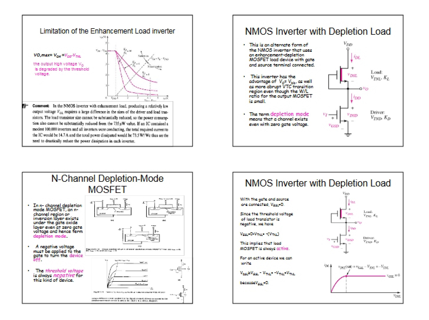
This resource is a focused exploration of NMOS inverter circuits, a fundamental building block in digital electronics. It delves into the practical considerations and performance characteristics of these circuits, specifically examining variations utilizing depletion-mode loads. The material builds upon core concepts of MOSFET operation and applies them to a key digital logic implementation. It’s designed for students seeking a deeper understanding beyond basic inverter theory.
Why This Document Matters
This material is invaluable for students in analog and digital electronics courses—particularly those tackling CMOS logic design. It’s most beneficial when you’re moving past introductory concepts and need to analyze the real-world behavior of circuits. It will help you understand the trade-offs involved in different inverter designs and prepare you for more complex circuit analysis and design projects. Students preparing for exams covering MOSFET circuits and digital logic will also find this a useful review and clarification tool.
Common Limitations or Challenges
This resource concentrates specifically on NMOS inverter limitations and doesn’t provide a comprehensive overview of all digital logic families. It assumes a foundational understanding of MOSFET physics and basic circuit analysis techniques. While it explores the characteristics of depletion-load inverters, it doesn’t cover alternative load implementations in extensive detail. It also doesn’t include step-by-step design procedures or simulation exercises; it focuses on conceptual understanding and analytical insights.
What This Document Provides
* Detailed examination of NMOS inverters employing depletion loads.
* Analysis of the operational characteristics and advantages of this specific inverter configuration.
* Discussion of key performance parameters and their relationship to circuit design.
* Exploration of the impact of device parameters on inverter behavior.
* Insight into the transition points and operating regions of the inverter circuit.
* Consideration of the relationship between input and output voltage characteristics.